StartUp Tools: Chip/Hardware Resources/Tools
We want to be the first investor in your hardware startup. Hardware startups require capital and hands-on expertise, so we blend the best elements of a seed stage firm and incubator....
Lemnos Labs is looking for passionate hardware entrepreneurs! You may be about to graduate from school, stuck at a large engineering firm, or may just....


Announcing the 2015 R/GA Accelerator
R/GA, the agency for the connected age, announces the second R/GA Accelerator, powered by Techstars, focused on startups in the Internet of Things (IoT) and Connected Devices space.
In partnership with:
Building on the success of its inaugural program, the second R/GA Accelerator is designed for startups developing connected hardware products and software services with the goal of helping them to build businesses and brands that can scale.
We have selected ten startups to join our three-month, immersive, mentor-driven program. The 10 companies reflect the fast growing realm of the Internet of Things that is powering connected devices - from homes and cars to warehouses and aircraft.
We are pleased to announce that companies selected into our upcoming program will receive support from world-class industrial design firm Astro Studios and PCH International, global leader in manufacturing and supply chain logistics, as well as industry leaders Stratasys, MakerBot and SOLIDWORKS.
The participation of these leaders in the IoT space combined with the support of R/GA's technology, product design and marketing talent provides startups in the program an incredible advantage over their competitors.
Our focus

The Internet has spilled out beyond the desktop and mobile screens and into devices, objects, and hardware. This isn't a passing fad, but a innovation that is quickly becoming a part of our everyday lives.
This massive shift in how we experience and harness technology, also called the "Internet of Things," includes new product categories, such as wearable technology and home automation and enterprise solutions.
The R/GA Accelerator taps into the emerging class of products that combine hardware, data, and digital services in compelling ways for consumers and businesses.
Demo Day 2015

At the conclusion of the R/GA Accelerator program our ten startups will pitch and showcase their companies at a one day invitation-only event in New York City. This past year, 650 investors, industry professionals and members of the media attended our R/GA Accelerator Demo Day 2014, after which many of the companies went on to meet or exceed their funding goals.
Get Connected




Create at your pace
Kick off your journey at a starting point which fits your current stage. If you're still bringing the pieces together, begin with Develop my hardware project and get resources to build your product. If you already have a strong working prototype and you're almost ready to launch, jump to Crowdfund my product to start pre-selling. Whether project or campaign, you've got a place to create your innovation with style.
Develop with Expert mentors
You've outlined your awesome idea, and you're eager to bring it to market. The Resource pool on HWTrek is a great knowledge base to assist you with making the next step. The Expert members found here have experience from all corners of the industry. Solicit advice from these mentors to plan the details of your product before diving into the execution process. It's this smart preparation that boosts your results.
Collaborate with ease
With your consolidated idea, it's time to source your parts and bring it all together. If you're the lone ranger type, take a DIY route to access the network of suppliers, designers and manufacturers and the Solutions they provide. Alternatively, you can team up with our personal project managers. They deliver a hands-on service to steer, connect and accelerate your project through the industry.
Project Development Hub
Your product is starting to take shape, now it's time to line up your path to market. Connect to the Project Development Hub to receive your customized production plan and additional resources for navigating production challenges. You'll be able to organize project tasks, integrate chosen Solutions into your schedule with ease, and keep your team in battle formation. It's management made easy.
Fund and deliver
Everything's come together into a strong working prototype and now it's time to hit the market. But with HWTrek, you hit the market running. Tap into venture capital connections, or launch your HWTrek crowdfunding campaign. This helps you fund your first manufacturing run, while growing your fanbase and media attention. Dispatch your orders, party, then clean up. You've got a business to run.
Showcase your business Solutions
Launching cutting-edge technologies and tapping into a world of innovation has never been easier. Create your Solution to present your hardware services and products. This gives you a visible space to display your brand identity and business focus the way you want. Just describe your component or service and connect it to the HWTrek marketplace.
Advance your media reach
Finding prospects at the right stage for partnership can take up valuable time and resources. With HWTrek, you can boost your reach to new leads in an innovative way. Build up your Expert profile and Solutions portfolio to let new Creator teams learn about your brand and the services you provide. Each Solution, update and message raises customer awareness of your brand, and your visibility on the Experts panel.
Collaborate with the next big thing
Your boosted reach lets you be found by new Creators, but that's only one half of the coin. HWTrek's sourcing network lets you be proactive and Discover early-stage projects which are looking for proposals. For additional leads, you can also speak to our sourcing and PM team to hop on our exclusive partner list.
Project Development Hub
The Project Development Hub helps you manage and track all your business partnerships from one space. Discuss specifications, update project schedules, oversee their development, and seamlessly integrate your Solutions into their production plans. This cloud-based tool gives you the oversight, and gives your partner the support to take products to market smoothly.
Market validation
Your business partnerships are coming to fruition, and now it's time to prepare for the large shipments you both want. Turn your prospects into clients, as they begin pre-selling products with a HWTrek crowdfunding campaign or tap into VC funding. This stage fires up production lines, and contributes to the market validation of your partnership - giving you the ability to forecast demand and plan ahead.

This month, I will be teaching a few MIT Media Lab graduate students and doing a bit of a "geek tour" of Shenzhen - we will visit several factories and live among the electronic markets to facilitate new directions and expand horizons in the students' hardware-oriented research projects.
As part of the course, they will learn how to scale up their research utilizing the China manufacturing ecosystem. These lessons may also be useful for Makers looking to bootstrap a product in moderate volumes (hundreds to thousands of units). I will share some tips and insights from the course in four posts over the next month covering:
- Getting a quotation: documentation standards (how to make a BOM)
- Process optimization: design for manufacturing and test jigs
- Industrial design for startups: guerrilla engineering on a shoestring budget
- How to pick a factory: building and maintaining partnerships
Part 1 of 4: The Quotation (or, How to Make a BOM)
Most Makers trying to scale up quickly realize the only practical path forward is to outsource production. If only outsourcing were as easy as schematic + cash = product! Whether working with the assembly shop down the street or going to China, a clear and complete bill of materials (BOM) is the first step to outsourcing production.
Every single assumption, down to the color of the soldermask, has to be spelled out unambiguously for a third party to faithfully reproduce a design. Missing or incomplete documentation is the lead cause of production delays, defects, and cost overruns. So, we will start the series on the topic of making a complete and accurate BOM for quotation.
Let's consider a simple case study. Suppose we Kickstarted a bicycle safety light. It contains a circuit using the 555 timer to flash a small array of LEDs. After a great marketing campaign, we now have to fill several hundred orders in a few months' time.
At this point, here's how the starting BOM might look:
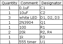
This BOM, along with a schematic, is likely sufficient for an engineer to reproduce the prototype, but this is far from adequate for a manufacturing cost quotation. Here's some of the things missing from the BOM:
- Approved manufacturer for each component
- Tolerance, material composition, and voltage spec for passive components
- Package type information for all parts
- Extended part numbers specific to each manufacturer
Furthermore, the table above addresses only the electronics BOM. A complete BOM for an LED flasher also needs to include the PCB, battery, plastic case pieces, lens, screws, any labeling (for example, a serial number), a manual, and packaging (plastic bag plus cardboard box, for example). There may also need to be a master carton as a single boxed LED flasher is too small to ship on its own. Although cardboard boxes are cheap, they aren't free, and if they aren't ordered on time, inventory will sit on the dock until a master carton is delivered for final pack-out prior to shipment.
Here's a little more about each of the missing items from the example BOM.
Approved manufacturersA proper factory will require the allowed manufacture(s) to be specified for every part. This is frequently referred to as the "AVL", or Approved Vendor List. A manufacturer is not a distributor (i.e., Digikey, Mouser, Avnet); a manufacturer is the actual company that makes the part. A capacitor, for example, could be made by TDK, Murata, Taiyo Yuden, AVX, Panasonic, Samsung, etc. You'll be surprised how many times I've reviewed a BOM listing "Digikey" or some other distributor as the manufacturer for a part.
While it may seem silly to trifle over who makes a capacitor, there are definitely situations in which the maker of a component matters - even for the humble capacitor. For example, blindly substituting the filter capacitors on a switching regulator, even if the substitute has the same rated capacitance and voltage, can lead to unstable operation and even boards catching fire.
Of course, there are times when one is truly insensitive to the manufacturer, in which case I would mark on the BOM "any/open" for the AVL (particularly true for things like pull-up resistors). This invites the factory to suggest their preferred supplier on your behalf.
Tolerance, composition, and voltage specFor passive components that are marked as "any/open", there are some key parameters that should always be specified in a BOM to ensure the right part is purchased:
- For resistors, at a minimum the tolerance and wattage should be specified. A 1k, 1% 1/4W carbon resistor is very different beast from a 1k, 5% 1W wirewound resistor!
- For capacitors, at a minimum the tolerance, voltage rating, and dielectric type should be specified. For special applications, certain parameters such as ESR or ripple current tolerance also need to be specified. A 10uF, electrolytic, 10% 50V capacitor has vastly different performance at high frequencies compared to a 10uF, X7R [ceramic], 20% 16V capacitor.
- Inductors are sufficiently specialized that it's not recommended to ever leave them as "any/open". For power inductors, core composition, DCR, saturation, temperature rise current, are the basic parameters, but there is also no standard for casing like there is for resistors and capacitors. Furthermore, important parameters such as shielding and potting, which can have material impacts on the performance of a circuit, are often implicit in a part number; hence, it's best to simply fully specify the inductor and not leave it any/open. The same goes for RF inductors.
It's always important to fully specify the form factor, or "package type", of a component. Poorly specified or under-specified package parameters can lead to assembly errors. Beyond the basic parameters such as the EIA or JEDEC package code (0402, 0805, TSSOP, etc.), here are some other things to consider:
- For SMT packages, the height of a component can vary, particularly for packages larger than 1206, or inductors. Pay attention if the board is slotting into a tight case.
- For through-hole packages, lead pitch and component height should always be specified.
- For ICs, try to specify the common name that corresponds to the package, not just the manufacturer's internal code (for example, a TI "DW" type package code corresponds to SOIC). It's a good consistency check that can guard against errors.
Designers often think using abbreviated part numbers. A great example of this is the 7404. The venerable 7404 is a hex inverter, and has been in service for decades. Because of its ubiquity, the term "7404" can be used as a generic term for an inverter. However, when going to production, things like the package type, manufacturer and logic family must be specified. A complete part number might be 74VHCT04AMTC, which specifies an inverter made by Fairchild Semiconductor, from the "VHCT" series, in a TSSOP package, shipped in tubes. The extra characters are very important, because small variations can lead to big problems, such as quoting and ordering the wrong packaged device (and subsequently being stuck with a reel of unusable parts), or subtle reliability problems. In fact, I encountered a problem once due to a mistaken substitution of a "VHC" for the "VHCT" logic family part. This switched the input thresholds of the inverter from TTL to CMOS logic-compatible, and resulted in some units having an asymmetric response to input signals. Fortunately, I caught this problem before production ramped, avoiding a whole lot of potential rework or worse yet, returns.
Here's another example of how missing a couple of characters can cost thousands of dollars. A fully specified part number for the LM3670 switching regulator might be LM3670MFX-3.3/NOPB. Significantly, if the /NOPB is omitted, the part number is still valid and orderable - but for a version that uses leaded solder. This could be disastrous for products exporting to a region, such as the EU, that requires RoHS compliance (meaning lead-free, among other things). A more subtle issue is the "X" in the part number. Part numbers with an "X" come with 3,000 pieces to a reel, and ones lacking an "X" come in 1,000 pieces to a reel. While many factories will question the /NOPB omission (since factories typically assemble RoHS documentation as they purchase parts), they will rarely flag the reel quantity as an issue. However, you care about the reel quantity because if you only wanted 1,000 pieces, including the X in the part number means you'll be paying for 2,000 extra pieces you don't need. Or, if you're doing a much larger production run and you omit the X, you could be paying a premium for shipping three times the volume of reels for the same purchase quantity. Either way, the factory will quote the part exactly as specified, and you could be missing out on a cost savings if you're not paying attention to the reel quantities.
The bottom line is that every digit and character counts, and lack of attention to detail can cost real money!
BOM RevisitedHere's an example of how a proper, fully-specified BOM for quotation of the same project example above would look.
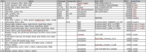
(click for a larger version, or get the original in open office format here)
Note that the BOM above doesn't call out factory margin, labor for assembly, pack-out, shipping, duties, etc. These "soft costs" will be discussed in the final post of the series. However, it's important to note that when building a business model, parts cost is not the only cost to consider - the above BOM just gets you started with the initial quotation process.
Let's compare this to our original BOM for contrast:

There is big difference between a BOM that any engineer could take to produce a prototype, and a BOM that any factory could take to mass-produce a product.
Note that two additional columns have crept into the final BOM, the "MOQ" (minimum order quantity) and the "lead time". These columns are irrelevant when building low-volume prototypes, as one would typically buy parts from distributors which have few MOQ restrictions and maintain stock on hand for next-day deliveries. However, when scaling into production, a big cost savings are realized by cutting the distributor overhead and buying through wholesale channels. In wholesale channels, MOQs and lead times matter.
The good news is the factory will fill in the MOQ and lead time as part of the quotation process. However, these are parameters that are helpful to be tracked from the beginning of a design. If the MOQ of a particular component is very high, one may have to buy massive numbers of excess parts which increases the effective price of the project. If the lead time of a part is very long, one may want to consider redesigning for a part with a shorter lead time. Using parts with shorter lead times not only saves time, it improves cash flow, as the last thing anyone wants to do is tie up cash on long-lead components 4 months in advance of any sales revenue.
Also note the inclusion of all the "miscellaneous" bits for the design inside the BOM, left out on the engineering prototype's BOM. The miscellaneous bits are easy to forget, but a missing user manual in an initial BOM is often times not discovered until opening the final sample for approval, leading to a last-minute scramble to get it into the final product. Many, many products have been delayed or late simply because a user manual or box art was not completed and approved in time, and it sucks to have a hundred thousand dollars worth of inventory idling in a warehouse for want of a slip of paper.
Finally, it's best practice to provide the factory with "golden samples" along with CAD files. These prototypes enable the factory to make smarter decisions about any ambiguities in the submitted BOM. It may suck to hand-solder together one more unit just for the factory, but in my opinion a few hours of soldering beats a week of trading clarifying emails with the factory.
Coping with ChangeDesigns change. Even if a design is perfect, sometimes vendors End-of-Life (EOL) components, forcing a change to the design. And let's face it, not all design assumptions survive contact with real consumers. While the quotation process is fluid, it's important to formalize the change process once crossing the threshold into production. It is best practice to use a written, formal Engineering Change Orders (ECO) to update the factory on any changes after the initial quotation is completed. An ECO template should have at a minimum the documentation detailing each part changed and brief explanation of why, along with a unique revision number for conveniently referencing the change down the road, and a method to record the factory's receipt of the ECO paperwork. Failing to be thorough about ECOs and relying on casual emails will often lead to buyers buying the wrong part, or worse yet the factory installing the wrong part and entire lots being scrapped or reworked. Even after troubleshooting a problem with the factory engineers, I will still write up a formal ECO and submit it to the production staff to formalize the findings. I hate paperwork as much as the next engineer, but in production one small mistake can cost tens of thousands of dollars, and that thought keeps me disciplined on ECOs.
Stay tuned for next week when I cover design for manufacturing and test jigs.
It's time to visit the topic of yield. This is a boring subject for many engineers, but as an entrepreneur your success or failure will be determined in part by achieving a reasonable yield. Unlike software, every copy of a physical good will have slight imperfections. Sometimes the imperfections will cancel out; and sometimes the imperfections gang up and degrade performance. As production volume ramps, these corner cases start adding up and a certain fraction of product ends up non-salable. In a robust design, the failing fraction may be so small that functional tests can be simplified, leading to further cost reductions. In contrast, designs sensitive to component tolerances will require extensive testing, and will suffer heavy yield losses. Reworking the defective units incurs extra labor and parts charges, ultimately leading to profit erosion.
Thus, a major challenge of moving from the engineering bench to mass production is re-designing to improve robustness in the face of normal manufacturing tolerances. This is called "design for manufacturing", or DFM.
Examples of tolerances to consider during the design process include:
- Passive component tolerances (i.e. resistance +/- 5%, capacitance +80/-20%, etc.)
Spec sheet parameters that vary widely (such as hFE for bipolar transistors, Vt for FETs, Vf for LEDs). Always read the datasheet and keep an eye out for parameters that have a wide min-max spread. For example, the min-max on hFE for Fairchild's 2N3904, ranges from 40 to 300, and the Vf on a superbright LED from Kingbright goes between 2 and 2.5V. - Voltage margins - particularly important for capacitors and input networks. As a rule of thumb, I try to spec capacitors with 2x headroom over nominal voltage, so I will try to use 10V caps for 5V rails and 6.3V caps for 3.3V rails. For example, many ceramic capacitor dielectrics reduce or derate their capacitance with increasing voltage. This means that ceramic capacitors in designs operating near their rated max voltage will see all the operating capacitances cornering toward the negative end of their tolerance range. Also, input networks - anything a user can plug something into - are subject to punishing ESD and other transient abuses, and special attention needs to be paid there to achieve the desired reliability.
- PCB trace widths and layer stack variations - impacts systems requiring matched impedance, or dealing with high currents.
- Mechanical tolerances - a case designed to fit a PCB with zero tolerance will result in the factory forcing PCBs into the case half the time, when either the PCB was cut a little large or the case came out a little small. This can lead to unintentional mechanical damage of the circuitry or the case.
- Cosmetic blemishes - any manufactured product is subject to small blemishes, such as dust trapped in plastics, small scratches, sink marks, and abrasions. It's important to work out the acceptance criteria for such defects ahead of time - i.e., not more than two dot blemishes larger than 0.2mm per unit, no scratch longer than 0.3mm, etc. so that the process can be crafted to avoid such defects, as opposed to the more expensive alternative of just building units and throwing away the ones that don't meet a set of criteria imposed late in the game. Of course, nothing comes for free - to do things on the cheap, avoid high-gloss finishes and consider using matte/textured finishes that naturally hide blemishes.
DFM Improves the Bottom Line
Let's return to our LED blinker case study from part 1 of the series. Let's say the prototype design calls for an array of three LEDs in parallel, each with its own current-set resistor. As noted above, Vf , the forward bias voltage of an LED at a given brightness, can vary by perhaps 20% between devices - in this case, from 2.0 to 2.5V. A design that uses resistive current limiting will amplify this variation. This is because an efficient circuit would drop a minority of the voltage across the current limiting resistor, leaving the parameter that sets the current - the voltage drop across the resistor - more sensitive to the variation in Vf. Since the brightness of an LED is proportional to the current flowing through the LED - not the voltage - the use of resistive current limiting to set LED brightness can lead to jarring inconsistencies in LED brightness uniformity.
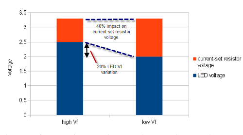
The above chart illustrates how a 20% LED Vf variation leads to a 40% change in the voltage across a current-set resistor for a fixed 3.3V supply, which will in turn lead to a 40% change in the current flowing through the LED, finally manifesting as a 40% change in perceived brightness.
Such a design may work well most the time - the problem is only pronounced when by chance a high Vf unit is paired with a low Vf unit. So for the one or two units prepared on the lab bench, things looked great.. However, a meaningful fraction of units may have brightness uniformities so bad there is choice but to reject the units. Given that most large hardware businesses have to survive on lean margins, losing even 10% of finished goods to defectivity is a terrible outcome.
One stop gap is to re-work the failed material. A factory can identify the LED that is too dim or too bright in an array, and replace it with a new one that may have a better chance of matching its cohorts. However, this rework drives up costs, and results in an unexpected and unpleasant invoice at the 11th hour of a manufacturing program. Naïve designers may be inclined to blame the factory for poor quality and argue over who should bear the cost, but it's better to proactively avoid these kinds of problems by subjecting every design to a DFM check, and using a small pilot run to sanity-check yield before punching out a whole bunch of units.
The cost of yield fallout quantifies how much money to spend on extra circuitry to compensate for normal component variability. For example, a $10 COGS product that is yielding 80% good units has an effective cost per salable unit of $12.5 (calculated using COGS x total units built / yielded units). Therefore, increasing the COGS by $2.5 to improve yield to 100% breaks even, and spending $1 to improve yield to 99% improves the bottom line by $1.38.
In the case of the LED flasher, the dollar could be spent on a current-feedback boost regulator IC, allowing the LEDs to be stacked in series instead of parallel, so that each LED is guaranteed to have a consistent and identical amount of current flowing through them, thereby leading to greatly improved lighting uniformity. While the cost of the boost regulator is much greater than the penny spent on three current limiting LEDs, the improvement in manufacturing yield more than pays for the extra component costs.
Test for Success
The other often-neglected responsibility of a designer is the test program. A factory can only detect the problems they are instructed to look for. Therefore, every feature must be tested, no matter how trivial. For example, on a chumby device, every user-facing feature had an explicit factory test - LCD, touchscreen, audio, microphone, all the expansion ports (USB, audio), battery, buttons, knobs, etc. etc. Even the simplest buttons had to be tested. While it's tempting to skip testing such simple components, I guarantee if it's not tested, it will lead to returns.
And no, do not outsource the test program to the factory, even if they offer the service. First of all, the factory often doesn't understand your design intent, so their test programs will either be inefficient, or they will test for the entirely wrong behavior. Also, factories have an incentive to pass as much material as possible, as quickly as possible, so factory-created test programs tend to be primitive and inadequate.
As a rule of thumb, for every product you make, you're actually making two related products: one for the end user, and a test for the factory. In many ways, the test for the factory has to be as user-friendly and foolproof as the product itself - after all, tests are not run by electrical engineers. However, the related testing product will be much quicker and faster to build if adequate testability features are designed into the consumer product.
Here are some guidelines when it comes to designing a test program:
- Strive for 100% feature coverage. It's often easy to overlook simple or secondary features - status LEDs, an internal voltage sensor, etc. As a sanity check, look at the device and list every way a consumer can interact with the device. Ask if the test program addresses every interaction surface, if even superficially - is every LED lit, every button pressed, every sensor stimulated and every memory device touched. If the product has a microcontroller, it's also helpful to review which drivers are loaded to cross-check the test list. Finally, do a schematic review and look at every port and consider key internal nodes to monitor as part of the test.
- Minimize incremental setup effort. In other words, optimize the amount of time required to set up the test for each unit. This is often done through jigs that employ pogo pins or pre-aligned connector arrays. A test that requires an operator to manually probe test a dozen test points or insert a dozen connectors is time consuming and prone to manual error. Most factories in China can help design the jig for a nominal cost, but jig design is easier and more effective if the design is provisioned with adequate test points.
- Automate test execution in a linear execution flow. Ideally, a test just run with a single button press, and then produce a pass/fail result. In practice, there will always be stop points that require operator intervention. An example of too much intervention is requiring an operator to key in or select an SSID from a list every time during a test for wifi connectivity. Instead, fix the test target SSID and hard-code that value into the test script so that the connection cycle is automatic.
- Use icons and colors to communicate with operators, not text. Not every operator is guaranteed to be literate in a given language.
- Employ audit logs. Record test results correlated to device serial numbers by incorporating a barcode scanner into the test rig. An alternative is to create a "test coupon" or a locally stored audit log to prove which units have had the test run successfully. This gives some hints as to what went wrong when a consumer returns a failed product. It also gives a quick method to check that the test procedure is being executed on all products. After an eight-hour shift of running test, an operator is prone to making mistakes, such as putting a defective unit accidentally into the good units' bin. Having a quick way to check that every product that ships has been subjected to and passed the full test can help identify and isolate such problems.
- Provide an easy update mechanism. Like any program, test programs also have bugs, and tests also need to evolve as the product has patches and upgrades applied . Thus it is imperative to have a mechanism to update and fix test programs without having to visit the factory every time in person. Many of my test fixtures have a mode where they can "phone home" via a VPN where I can then ssh into the jig itself to fix bugs: even my simplest jigs employ a linux laptop at its core.
The guidelines above are easy to implement if the product is designed with testability in mind. As most of the products I design run Linux, I leverage the processor inside the product itself to run the majority of the tests and manage the test UI. For products that lack user interaction surfaces, I will use an Android phone or a laptop connected via wifi or serial as the test UI.
Testing vs. Validation
Production tests are meant to check for assembly errors, not parametric variations or design issues. If a test is screening out devices because of normal parametric component variations, either buy better components, or re-do the design.
For consumer-grade products, there is no need to run a five minute comprehensive RAM test on every unit - in theory, a product should be designed well enough that if it's all soldered together correctly, the RAM will do its job. A quick test to check that there are no stuck or open address pins is all that is really need. Name-brand chip vendors have typically very low defectivity rates, so we're not validating the silicon; rather, we are validating the solder joints, connectors, and checking for missing or swapped components (note that if you buy clone chips or off-brand/remarked/partially tested devices to cut costs, it is advised to make a mini-validation program for those components).
To illustrate the point, let's consider testing vs. validation for a switch.
A production test for a switch on a product may simply consist of asking the operator to hit the switch a few times and verify that the feel is right.
A validation test for a switch may consist of taking a few devices, measuring contact resistance with a five-digit multimeter, subjecting them to 100% humidity at 40C overnight, and then putting the devices into an automated jig where the switches are cycled ten thousand times. Finally, the switches are re-measured with a five-digit multimeter and any degradation in close-state contact resistance is noted.
Clearly, this level of validation cannot be performed on every device manufactured. Rather, the validation program checks for performance of the switch over the expected lifetime of the product, and the test just makes sure the switch is put together right. Note that it is considered good practice to re-run validation tests on a couple randomly sampled units out of every several thousand units produced; there are formulas and tables to compute how much sampling is needed to achieve a certain level of quality.
So how much testing is enough testing? One threshold for testing can be derived through a cost argument. Every additional test run incurs test equipment costs, engineering costs, and the variable cost of the test time. As a result, testing is subject to diminishing returns: at some point, it's cheaper just to take a product return than to test more. Naturally, the testing bar is much higher for medical or industrial grade equipment, as the liability associated with faulty equipment is also much higher. Likewise, a novelty product meant to be given away may get away with much less testing.
As a final thought, don't dismiss the value of applying solid engineering to test jig design. I once had a problem once where a flat flex cable adapter with 50 pins had random cold solder joint failures. I asked the factory to build a test to validate the adapters. Their solution was to hang LEDs off of every pin of the adapter and put a test voltage into one side, and look for LEDs that don't light up on the other side. The problem is that the cold solder joints weren't simply open or closed - some were just high resistance. Enough current would flow to light an LED, yet enough resistance would be present to cause a fault in the design. After I noted this problem, the factory proposed buying 50 multimeters and hanging them off of every pin to check the resistance manually - an expensive and error-prone proposition. My response was to daisy-chain the connections across the adapter, and then use a single multimeter to check the net resistance of the daisy chain. Putting the connections in series checks all 50 connections with a single numeric measurement (as opposed to the subjective observation of an LED's brightness). As one can see, even a test as simple as checking for cold solder joints on a cable adapter can have better or worse implementations. As ever more complicated components require ever more subtle tests, there is real value in applying solid engineering skills to crafting efficient yet foolproof tests.
Sex sells. The performance of a CPU or amount of RAM in a box, to within a factor of two or so, is less important to a typical consumer than how the device looks. Apple devices command a hefty premium in part because of their slick industrial design, and many product designers aim to emulate the success of Sir Jony Ives in their own products.
There are many schools of thought in industrial design. One school invokes the monastic designer, coming up with a beautiful, pure concept, and the only thing the production engineers can do is spoil the purity of the design. Another school invokes the pragmatist designer, working closely with the production engineers, hammering out gritty compromises to produce an inexpensive and high-yielding design.
In my experience, neither extreme is compelling. The monastic approach often results in an unmanufacturable product that is either late to market or exorbitant to produce. The pragmatist approach often results in in a cheap look and feel, to which consumers have trouble assigning a significant value. The real trick is understanding how to strike a balance between the two.
Trim and finish are difficult, and therefore a point of distinction when it comes to design. The current design fad is minimalism, with an emphasis on "honest" finishes. An honest finish features the natural properties of the material systems in play, and eschews the use of paints and decals. Minimalist, honest designs are very hard to manufacture. Minimal designs have...well, minimal, features - and as a result even tiny blemishes stand out. Honest finishes likewise can be very difficult, as an honest finish means no paint: all the burs, gates, sinks, knits, scoring and flow lines that are a fact of life in manufacturing are laid naked before the consumer. As a result, this school of design requires well-made tools that are constantly checked and maintained throughout production.
If you don't have pockets deep enough to invest in new equipment and capabilities on behalf of your factory (i.e., if you're not a Fortune 500 company), the first step is to learn the vocabulary available. A design vocabulary is defined by the capabilities of the factory or factories producing the goods. What materials, what finish, what tolerances are achievable, what fastening technology is available - these are all heavily dependent upon the processes available.
Therefore, I find that visiting a factory in person early in the design process results in a better design result. In a factory visit, some design vocabulary will be discarded, but some new vocabulary will be discovered as well - the engineers who work the factory day in and day out develop process innovations that can open up novel design possibilities that are not knowable without the on-site visit.
The chumby One contains a concrete example of the impact manufacturing process can have on design outcome. In the original concept art, the blue highlight around the front edge was added to evoke the feeling of a speech balloon, like those used in captioning comics - the idea being the chumby is captioning your world with snippets from the Internet.
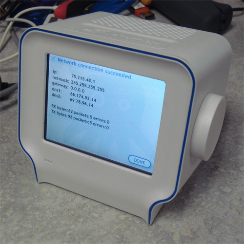
It turns out the implementation of such a blue trim across a raised surface is very hard. At the first factory, we implemented the highlight using paint. Silk screening was not an option because the shape wasn't flat enough. Pad printing can handle curved surfaces, but the alignment wasn't good enough, as the tiniest bleed over the edge looked terrible from the side. Decals and stickers likewise could not achieve the alignment required. In the end, a small channel had to be carved to contain the paint, and a stencil plus spray paint process was employed to create the highlight. The yield was terrible - in some lots, over 40% of the cases were being thrown away due to painting errors. Fortunately, plastic is cheap, so throwing away every other case after painting had a net cost impact of about $0.35.
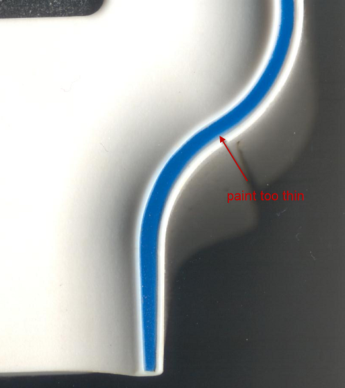
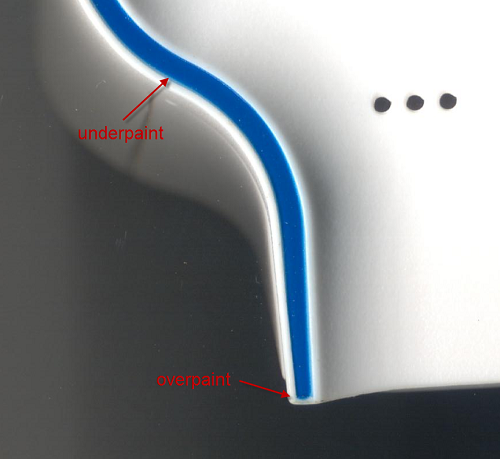
Mid-way through production, we migrated to a second source facility. They had a different plastic molding capability, and unlike the first factory, the second facility could do double-shot molds. Double-shot molds have twice the number of tools, but they can injection mold two different colors, or even different materials, into the same mold. Thus, at the new factory, we opted to use a double-shot process for the thin blue strip, instead of painting. The results were stunning. Every unit came off the line with a sharp, crisp blue line; and no paint meant a more honest, clean finish. However, the cost per case jumped to $0.94 a piece due to the more expensive process, despite the 100% yield. In fact, it would be cheaper to throw away more than half of the painted cases, but even the best painted cases could not compare to the quality of the finish delivered by the double-shot tool.

Another great example of how tweaking a factory process can improve a product's appearance is the Arduino motherboard. The wonderfully detailed artwork on the back side, sporting an outline of Italy and very fine lettering, isn't silkscreen. They actually put on two layers of soldermask, one blue, and one white. Because soldermask is applied using a photolithographic process, the resolution, consistency and alignment of the artwork is much better than a silkscreen. And since an Arduino's look is the circuit board, it gives the product a distinctive high-quality look that is difficult to copy using conventional processing methods.
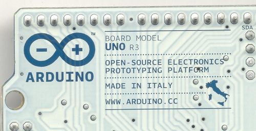
Thus, the process capability of the factory - painting vs. double-shot molding, double soldermasking vs. silkscreening - can have a real effect in the outcome of a product's perceived quality, without a huge impact on cost. However, a factory may not appreciate the full potential of their processes, and so it requires a designer's direct interaction to realize the potential. Unfortunately, many designers don't visit a factory until something has gone wrong, at which point the tools are cut and even if they see a cool process that could solve all their problems, it's often too late.
Design is an intensely personal activity, and as a result every designer will develop their own process. This is the general process I might use to develop a product on a tight, startup budget:
- 1. Every design starts with a sketchbook. First, decide on the soul and identity of the design, and pick a material system and vocabulary that suits your concept. But don't fall in love with it...
2. Break the design down by material system, and identify a factory capable of producing each material system.
3. Visit the facility, and take note of what is actually running down the production lines. Don't get too drawn in by the sample room or one-off bits. Practice makes perfect, and from the operators to the engineers they will do a better job of executing things they are doing on a daily basis than reaching deep and exercising an arcane capability.
4. Re-evaluate the design based on a new understanding of what's possible, and iterate. This may require going back to step 1, or it may just require small tweaks. But this is the stage at which it's easiest to make compromises without sacrificing the purity of the design.
5. Rough out the details of the design - pick parting lines, sliding surfaces, finishes, fastening systems, etc. based upon what the factory can do best.
6. Pass a revised drawing to the factory, and work with them to finalize details such as draft angles, fastening surfaces, internal ribbing, etc.
7. Validate the design using a 3D print and extensive 3D model checks.
8. Identify features prone to tolerance errors, and trim the initial tool so that the tolerance favors "tool-safe" modifications. For example, in injection molding it is easier to remove steel than to add it to a tool, so target the initial test shot to have less plastic than too much on critical dimensions. A button is an example of a mechanism that benefits from tuning: it's hard to predict from CAD or 3D prints exactly how a button will feel, and getting that tactile feel just perfect usually requires a little trimming of the tool.
Just like the wands from Harry Potter, a good factory chooses you as much as you choose them. Forget the term "vendor" and replace it with "partner": if you're doing it right, you aren't simply instructing the factory; there should be a frank dialog about the trade-offs involved, and how things can be improved. Furthermore, a healthy relationship with a factory can lead to better payment terms, which improves cash flow. In some cases, factory credit can directly replace raising venture capital, taking loans, or Kickstarting. As a result, I treat good factories with the same respect as investors and partners in a business.
Here are some basic things to remember when forming a relationship with a factory.
- "It's easy to know the cost, but hard to know the price". Cost reduction is critical for any business, but nobody can make up a loss with volume. When negotiating prices with a factory, take a step back and check if everything makes sense. If a quote seems too good to be true, it often is. Factories that lose money on a deal will stop at no end to make it back. Many manufacturing horror stories have roots in unhealthy cost structures - a factory's first prerogative is survival, even if it means mixing defective units into lots to boost margin, or assigning novice engineers to a flagging project to better monetize their seasoned engineers on more profitable customers.
- "If you can't talk with the boss, you're nobody". Work with a factory too big, and you risk getting lost in bureaucracy, and pushed out of the line at critical times by bigger customers. Work with a factory too small, and they can't provide the services you need. My rule for right-sizing a factory is to pick the biggest facility where you can get direct access to the lao ban (factory boss) on a regular basis. It's a good sign if on the first meeting, the lao ban is there to give you a tour and asks astute questions about your business over lunch.
- "Light is the best disinfectant". If a factory will not quote with an "open BOM", i.e., a quotation where the cost of every component, process, and margin is explicitly disclosed (not the same use of the word "open" as in the F/OSS context), I won't work with them. Cost reduction discussions cannot function without transparency; there are too many places to bury costs otherwise. Likewise, if cost discussions seem to be turning into a game of "whack-a-mole" where reduced costs on one line item are inexplicably popping up in another item, run away.
A quote should have called out the price of each part, the excess for the job, labor, overhead, and NRE. Here are some of the fine points to understand about quotations that are not immediately obvious:
- "Excess" is the result of what I call the hot dogs-and-buns problem. Hot dogs come in packs of 10, but buns come in packs of 8. So unless one buys 40 servings, there's going to be left over buns or hot dogs. Likewise, many components come only in 3,000 piece reels, so a 10,000 piece build will conclude with 2,000 pieces of excess (four reels equals 12,000 pieces). "Cut tape" (or partial reels) exist, but the cost per part of cut tape is much higher, as this just shifts the risk of excess material onto the distributor. Excess isn't all bad - excess can be folded into future runs of a product. So, as long as a decent run rate is sustained, the excess inventory turns into cash on a regular basis. However, at some point production will end or pause, and the bill for the excess will arrive, putting a crimp on cash flow. If a quote is lacking an excess column, it's possible the factory is charging for the full reel but keeping the excess for their own purposes (this is where many of the gray market goods in Shenzhen come from); or they will just send an unexpected invoice for it down the road. In my opinion, it's best to get that all out there up front so as to build a complete cradle-to-grave business model.
- Labor costs are devilishly tricky to estimate. However, the good news is that for high tech assemblies, labor is typically a small fraction of total cost. The labor cost of assembling a straightforward board with 200 parts on it in small volumes in China may be about $2-3, whereas the cost of doing it in the US is closer to $20-$30. So even if labor prices double overnight in China and halve in the US, China may still be competitive. This is in contrast to the lower-value goods moving out of China (such as textiles), where the base value of the raw material is already low so labor costs are a significant portion of the final product cost. I usually don't argue too much over labor costs, since the end result of scrimping on labor is often lowered quality, and pushing too hard over labor costs can force the factory to reduce the worker's quality of life by trimming benefits.
- Factory margin is also a bit of an art to negotiate. The fair margin for a factory depends on how much value they've added, and the volume of production. There are no hard and fast rules for margin. Although I give guidance here, remember there are always exceptions to the rule, and everyone has a special deal that can be cut. Also, the definition of "margin" varies depending on the facility. Some facilities include scrap, handling overhead, and even R&D expense into the "margin", whereas others may break those out on separate lines, so it's important to look at the big picture and use some common sense when reviewing a quotation. In general, margin will range between single-digit to low double-digit percentages depending upon volume, value add and project complexity. For very low quantity production lots (~1k pieces) there may also be a per-lot "line fee" charged. This fee partially defrays the cost of setting up an assembly line only to tear it down after running for a short period of time. A line's throughput may be very fast, producing hundreds to thousands of units a day, but it also takes days to set up.
- NRE, or "non-recurring engineering" - these are one-time fees required to set up a production run, such a stencils, SMT programming, jigs and test equipment. Note that the re-use of test equipment between customers is considered bad practice, so if a multimeter is required as part of a production test, don't be surprised if a bill for a multimeter is tacked onto the NRE. This is due to customers having drastically varying standards around the maintenance and use of test equipment.
Here are a few final parting thoughts to keep in mind.
- Have an understanding of how scrap or exceptional yield loss is handled. There are a few schools of thought around this. Ideally, one only pays for good, delivered items, and the factory bears the burden of defectivity. This gives the factory an incentive to maintain a high production quality, because every percent of defectivity eats away at their margin. However, if the design has a flaw or is too hard to build, and defectivity is high, the factory may start shipping lower quality units as a desperate measure to meet production and margin targets. They may also start gray-marketing defective goods to recover cost, leading to brand reputation problems down the road. It's good to have some sort of an understanding on how to handle such a contingency ahead of time. This may include, for example, a dedicated "scrap" line item inside the quotation to handle defectivity explicitly.
- On the subject of scrap & yield, it's a good idea to order more units than the proven demand. These extras go toward handling returns and exchanges. Despite best efforts, mistakes do happen; sometimes they aren't your fault, such as shipping damage. Ordering 1,000 pieces to fulfill a 1,000 piece Kickstarter campaign means returns and exchanges can be handled with only refunds, as it's just not practical to fire up the factory to make a dozen replacement units. Thus, as a general rule, I order a few percent excess beyond the customer deliverable, so that I have stock on hand to handle returns and exchanges. Units that don't get used up by the returns process then turn into demo loaners or business development give-aways to drum up the next set of orders!
- Keep an eye on shipping costs. These fees aren't typically built into a quotation, but they impact the bottom line (greatly so for low-volume products). Fedex is a great tool to save time, but it's also a very expensive addiction. Courier fees can easily wash out the profit on a small project, so manage those costs. Pro tip: couriers will offer discounts to frequent shippers, but you have to call in to negotiate the special rates.
- Duties. Keep in mind that components imported to China without an import license are levied a 23% or so automatic duty on their value. The general rule for China is dutiable on import, duty free on export. If stuff is accidentally shipped across the border to Hong Kong, expect to pay a duty to get it back into China. Customs brokers can work the angles - for example, some brokers can get goods taxed by their weight and not their value, which for microelectronics is typically a good deal. I haven't figured out all the customs rules, as they seem to be a moving target - every month it seems there is a new rule, fine, exceptional fee or tariff to deal with. There are also plenty of shady ways to get goods into China, but I sleep better at night knowing I do my best to comply with every rule. The reason quotations don't include duties is that it's assumed by default there will be an import license. Import license enable the duty-free import of goods. However, import licenses cost a few thousand bucks, take weeks to process, and have no room for flexibility, as they are tied to an exact BOM for the product. Small ECOs can invalidate a license - customs officers are known to count the number of decoupling caps on a PCB, and if it doesn't match the count in the license, a fine is levied and the license is invalidated. Even deviations in the material used to line the decorative box can invalidate a license. This import license scheme favors high-volume produces, and punishes low volume producers.
As one can see, going to China isn't for everyone. Particularly for those based based in the US, the overhead of courier fees, travel, duties, and late-night concalls adds up rapidly. As a rule of thumb, a US designer is better off assembling PCBs in the US for volumes less than 1k, and they don't start seeing clear advantages until perhaps 5k-10k volumes. That math shifts in China's favor as processes such as injection molding and chassis assembly come into play, due to the immense amount of expertise China has accumulated in these labor-intensive processes. Also, the break-even point can be much lower for those living in or near China, as courier fees, travel, and time zone impact are all a small fraction of what they are coming from the US. This compounds with the fact that locals are more effective at leveraging the component ecosystem in China, leading to further cost reductions compared to a design produced using only parts available in the US ecosystem. On the other hand, physically large assemblies or systems built using lots of dutiable components may be cheaper to build domestically, as it saves on shipping costs and tariffs. In the end, one should keep an open mind and try to consider all the possible secondary costs and benefits of domestic vs. foreign production before deciding where to park production.

Click a checkbox to disable a supplier.
Drag a supplier box onto another to exchange priorities.
Optimization changes suppliers and may round up quantities to the nearest price break.

From the Blog

Following the manufacturing process of the PCBs we can perform a visual inspection in order to find any problems with a board. That works fine for a two layer pcb. For multi-layer PCBs... Read More
Custom Quote
Require large quantities, high layer counts
and/or more flexibility and control? Let us
provide you with a custom quote.
Buy Now
Instant pricing and ordering for 2 to 6 layer prototype printed circuit boards. Faster service, less design flexibility.
Free PCB Design Software
PCB Creator makes printed circuit
board design fast and easy.


Home " PCBexpress Quickturn Quoting

Do you have a simple PCB job that you need completed in a hurry? Our PCBexpress ® Quickturn printed circuits service is your best option. We offer:
Reset Form / New QuoteGeneral Board InformationDimensions inches

This is the X and Y axis measurement in inches.
The largest dimensions available for FR4 boards is 12 x 14 in. The largest dimensions available for Rogers 4350 boards is 8 x 8 in. The smallest board dimension is 0.25 inches in one direction.
For different sizes please use our Full Featured quote page.
Email Address
Please enter your email address to receive an online quote.
Privacy PolicyBoard Material
Surface Finish
This is the plating finish that will be deposited over the copper. Quick Turn surface finishes include silver and tin lead.
Also referred to as Legend or Nomenclature - usually contains component placement & component designators. White Silkscreen available for Quick Turn Products.
Slots/Cutouts

Any internal area being removed is a cutout. This field is required for all internal slots so that we properly account for them.
When the board outline has a notch measuring less than .062" we count that notch as a cutout due to the tool change needed to negotiate the smaller areas.
Not Limited To Circles or Squares
Native File Upload
We can assist in the export of Gerber 274X and NC Drill files from Ivex Winboard, Altium/Protel, EAGLE or OrCAD files.
We also have DFM rule sets for Altium Designer and EAGLE CAD software on our downloads page.
These tools will assist in ensuring manufacturability of your boards at Sunstone Circuits.
Assembly
Expedite
Choose 1 Day Expedite to save 1 day lead-time. Choose Double Expedite to save 2 Days.
1 Day Expedite is available for 2, 4, and 6 layer boards with solder mask. Double Expedite is avaliable for 4 layer boards.
* Fabrication notes will not be reviewed for Quickturn service






When leaving a parking garage have you ever wondered how the gate knows how to close only after you have pulled out? The magic lies below the concrete, there is an inductive loop in the ground under the gate arm. It sensed the presence of your car and lets the gate close only once your car can no longer be detected. You can also see these loops used in modern intersections to control the traffic lights as efficiently as possible, for example when there are no cars in the turn lane there is no need to waste 30 seconds flashing the turn arrow while holding back the through traffic.
Thanks to our friend Muris for creating a DIY Inductive Loop Vehicle Present Sensor and providing all the details so you can build your own or modify the design for your own needs. It has a PIC16F877A to control the show and has a ton of adjustability so it can be used for almost any situation.
" Specifications
- Tuning: Automatic
- Detection type: Presence/Pulse
- Presence time: Adjustable in 4 steps (default: 11 min, 33 min, 55 min, infinity)
- Pulse duration: 100 ms / 500 ms
- Signal filtering: Adjustable in 4 steps (LOW, MED-LOW, MED-HI, HI)
- Coil/loop inductance: 20 uH - 1000 uH
- Frequency range: 40 kHz - 140 kHz
- Frequency adjustment: 4 steps (LOW, MED-LOW, MED-HI, HI)
- Sensitivity: 0.001\% - 0.5\% digital in 8 configurable steps
- Detection speed: <10 ms (with LOW filtering stage and loop frequency of 40 kHz)
- Startup time: ~8 sec
- Power supply: 7-40 V DC / 5-28 V AC
- Current consumption: ~0.035 A
- Protection: Galvanic isolation + gas discharge tube for lightning protection"


From February 1, 2014 to March 1, 2014, in partnership with TI/BeagleBone Adafruit will be giving away 10 BeagleBoneBlack cases per week, all you need to do is share your project and we'll pick 10 a week for 4 weeks! Share a photo or video of your BeagleBone Black project on Flickr ( Read More ...
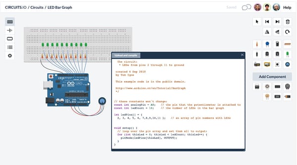
What Arduino can do
Arduino can sense the environment by receiving input from a variety of sensors and can affect its surroundings by controlling lights, motors, and other actuators. The microcontroller on the board is programmed using the Arduino programming language (based on Wiring) and the Arduino development environment (based on Processing). Arduino projects can be stand-alone or they can communicate with software running on a computer (e.g. Flash, Processing, MaxMSP).
The boards can be built by hand or purchased preassembled; the software can be downloaded for free. The hardware reference designs (CAD files) are available under an open-source license, you are free to adapt them to your needs.
Arduino received an Honorary Mention in the Digital Communities section of the 2006 Ars Electronica Prix. The Arduino founders are: Massimo Banzi, David Cuartielles, Tom Igoe, Gianluca Martino, and David Mellis. Credits
Buy an Arduino Board
Buy an Arduino Board from the official Arduino store or from one of the authorized Arduino distributors world wide.
Download the Arduino Software
The Arduino Software is free, open source, and available for Windows, Mac OS, and Linux.
Getting Started
Visit Getting Started for specific instructions for your operating system and your board. If you're having trouble, check out the troubleshooting suggestions.
Support
The official Arduino multi-language forum is the place to start with questions of all kinds.
Development
For information on the development of Arduino, see the Arduino project on GitHub. Changes to the software are discussed on the developers mailing list.
Contact Us
Contact us to get answers to your comments and questions. Make sure you select the right email address from the list of topics.
Arduino Day 2014
Arduino Day is a worldwide celebration of Arduino's first 10 years. It's 24 hours full of events - both official and independent, anywhere around the world - where people interested in Arduino can meet, share their experiences, and learn more.
Community
The community of Arduino enthusiasts is vast, and includes region specific groups and special interest groups. The community is an excellent further source of support on all topics such as accessory selection, project assistance, and ideas of all sorts.
The Arduino Wiki (Playground) is a collection of Arduino knowledge, tutorials, and instructions provided directly by Arduino users.
Check out the official Arduino multi-language forum and stay connected with the Arduino community:
